

Review Article
Volume-1 Issue-1, 2026
Effect of Annealing Treatment Atmosphere on the Structural and Optical Properties of Silver Doped Zinc Oxide Thin Films
-
Received Date: February 05, 2026
-
Accepted Date: February 20, 2026
-
Published Date: February 22, 2026
Journal Information
Abstract
In this work, the effect of annealing atmosphere on structural and optical properties of silver-doped ZnO thin films (SZO) have been investigated. Silver-doped zinc oxide thin films (SZO) deposited onto glass substrates are synthesized using sol– gel technique via spin coating. XRD analysis reveals that the Ag incorporation leads to a decrease in grain size in ZnO: Ag thin films annealed in air and under nitrogen atmospheres. Conversely, an increase in grain size was noticed for Ag doped ZnO thin films annealed under oxygen flow. All films are highly transparent in the visible region for different annealing treatment environment. In addition, band gap energies were found to decrease after Ag doping as compared to those of pure ZnO thin films post-annealed in different atmospheres. As compared to pure ZnO thin films, an increase of the photoluminescence intensity was noticed.
Key words
ZnO thin films, Sol-gel, Annealing Treatment Atmosphere, Silver-Doping
|
Results JCPDS (pure powder ZnO) |
Experiment: Ag content Ag/Zn (%) |
|||
0 |
1 |
2 |
3 |
||
2θ (°) |
|
|
|
|
|
(002) |
34.422 |
34.464 |
34.458 |
34.462 |
34.448 |
(101) |
36.253 |
36.288 |
36.290 |
36.285 |
36.279 |
doo2 [Å] |
2.603 |
2.600 |
2.600 |
2.600 |
2.601 |
d101[Å] |
2.475 |
2.473 |
2.473 |
2.473 |
2.4740 |
a[Å] |
3.249 |
3.246 |
3.246 |
3.247 |
3.2474 |
c[Å] |
5.206 |
5.2 |
5.201 |
5.200 |
5.202 |
c/a |
1.602 |
1.601 |
1.602 |
1.601 |
1.602 |
L[Å] |
1.977 |
1.975 |
1.975 |
1.975 |
1.976 |
Volume of unit cell |
47.6 |
47.471 |
47.471 |
47.483 |
47.510 |
D[nm] |
|
44.380 |
26.559 |
34.047 |
31.223 |
s (10-4) |
|
26.363 |
44.060 |
34.366 |
37.749 |
∫ [lines/m2] *1014 |
|
5.077 |
14.175 |
8.626 |
10.257 |
|
Results JCPDS (pure powder ZnO) |
Annealing treatment under nitrogen flow |
|||
0 |
1 |
2 |
3 |
||
2θ (°) |
34.422 |
34.432 |
34.459 |
34.460 |
34.461 |
doo2 [Å] |
2.603 |
2.602 |
2.600 |
2.600 |
2.600 |
a[Å] |
3.249 |
3.249 |
3.246 |
3.244 |
3.244 |
c[Å] |
5.206 |
5.204 |
5.200 |
5.200 |
5.200 |
c/a |
1.602 |
1.601 |
1.602 |
1.603 |
1.602 |
L |
1.977 |
1.977 |
1.975 |
1.974 |
1.974 |
Volume of unit cell |
47.62 |
47.595 |
47.458 |
47.406 |
47.416 |
D[nm] |
|
29.359 |
21.135 |
24.338 |
25.533 |
s (10-4) |
|
39.887 |
54.873 |
48.079 |
45.829 |
∫ [lines/m2] *1014 |
|
11.601 |
22.385 |
16.881 |
15.338 |
|
Results JCPDS (pure powder ZnO) |
Annealing treatment under Oxygen flow |
|||
0 |
1 |
2 |
3 |
||
2θ (°) |
34.422 |
34.448 |
34.602 |
34.467 |
34.454 |
doo2 [Å] |
2.603 |
2.601 |
2.59 |
2.599 |
2.600 |
a[Å] |
3.249 |
3.247 |
3.235 |
3.245 |
3.246 |
c[Å] |
5.206 |
5.202 |
5.18 |
5.199 |
5.201 |
c/a |
1.602 |
1.602 |
1.601 |
1.602 |
1.602 |
L[Å] |
1.977 |
1.976 |
1.968 |
1.974 |
1.975 |
Volume of unit cell |
47.62 |
47.505 |
46.952 |
47.418 |
47.477 |
D[nm] |
|
27.635 |
23.824 |
37.859 |
30.671 |
s (10-4) |
|
42.357 |
48.919 |
30.902 |
38.158 |
∫ [lines/m2] *1014 |
|
13.094 |
17.617 |
6.976 |
10.630 |
|
Silver doping % |
||||
0 |
1 |
2 |
3 |
||
Eg((eV) |
Annealing treatment in air |
3.247 |
3.237 |
3.242 |
3.225 |
Annealing treatment under nitrogen |
3.248 |
3.225 |
3.236 |
3.25 |
|
Annealing treatment under oxygen |
3.29 |
3.268 |
3.238 |
3.258 |
|
[Ag/Zn] % |
Eg(Opt)[eV] |
UV peak positon |
Eg(PL) [eV] |
|
Annealing treatment inair |
0 |
3.247 |
394.708 |
3.142 |
1 |
3.237 |
380.739 |
3.258 |
|
2 |
3.242 |
379.261 |
3.2708 |
|
3 |
3.225 |
377.642 |
3.284 |
|
Annealing treatment under nitrogen flow |
0 |
3.248 |
379. 821 |
3.266 |
1 |
3.225 |
381.193 |
3.254 |
|
2 |
3.236 |
378.665 |
3.275 |
|
3 |
3.25 |
378.043 |
3.281 |
|
Annealing treatment under oxygen flow |
0 |
3.29 |
377.642 |
3.284 |
1 |
3.268 |
380.37 |
3.261 |
|
2 |
3.238 |
378.043 |
3.281 |
|
3 |
3.258 |
378.445 |
3.277 |
|
 |
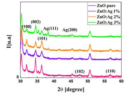
| Figure 1: XRD patterns of pure and Ag doped ZnO thin layers deposited onto glass substrates and annealed in air |
 |
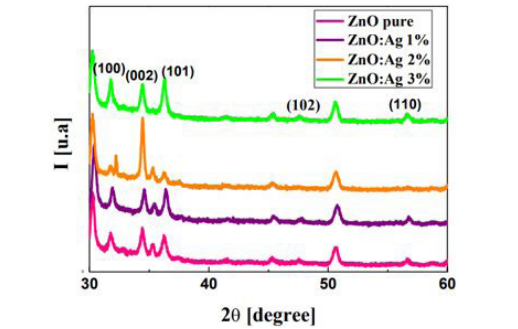
| Figure 2: XRD patterns of pure and Ag doped ZnO thin layers deposited on glass substrates and annealed under nitrogen flow |
 |
| Figure 3:XRD patterns of pure and Ag doped ZnO thin layers deposited on glass substrates and annealed under oxygen flow |
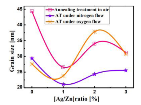 |
| Figure 4: Variation of the grain size with various Ag doping concentrations for thin films post annealed under different environment of annealing treatments |
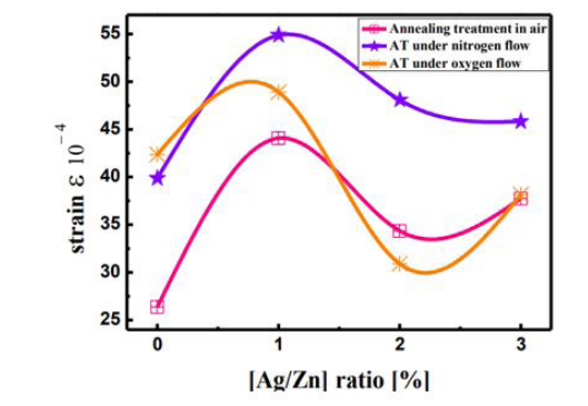 |
| Figure 5: Variation of the strain in ZnO and ZnO:Ag films annealed under different environments of annealing treatments |
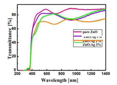 |
| Figure 6: Transmittance spectra of SZO thin films annealed in air |
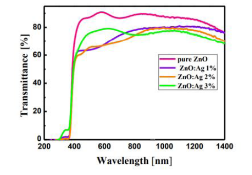 |
| Figure 7: Transmittance spectra of Silver-doped ZnO thin films annealed under nitrogen flow |
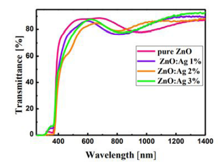 |
| Figure 8: Transmittance spectra of silver-doped ZnO thin films post-annealed under oxygen flow |
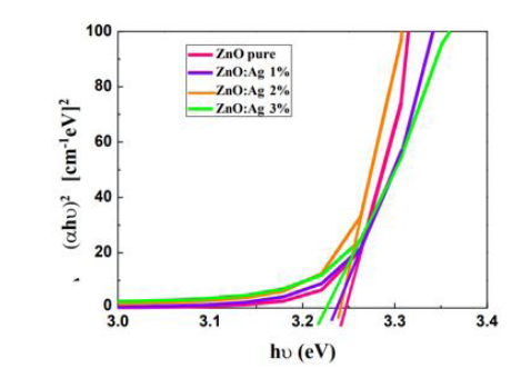 |
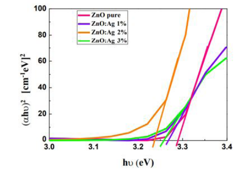
| Figure 9: Plots of ((??????) vs. photon energy ???? of Ag-doped ZnO thin films annealedin air |
 |
| Figure 10: Plots of (??????) vs. photon energy ???? of silver-doped ZnO thin films annealed under nitrogen flow |
 |
| Figure 11: Plots of ((??????) vs. photon energy ???? of silver-doped ZnO thin films annealed under oxygen flow |
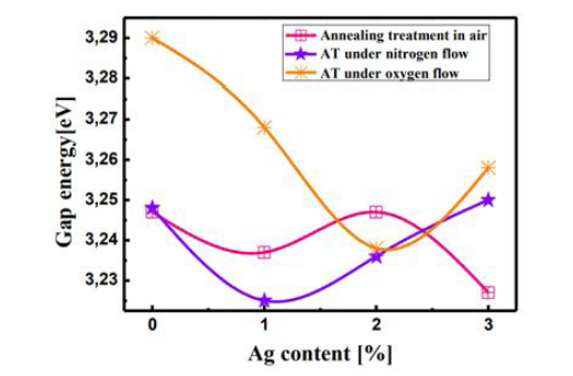 |
| Figure 12: Plots of gap energy vs various Ag doping concentrations annealed under different atmospheres |
 |
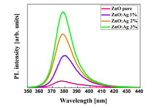
| Figure 13: Photoluminescence spectra of ZnO:Ag thin films vs wavelength annealed in air atmosphere |
 |
| Figure 14: Photoluminescence spectra of ZnO:Ag thin films vs wavelength annealed under nitrogen flow |
 |
| Figure 15: Photoluminescence spectra of ZnO: Ag thin films vs photon energy annealed under oxygen flow |
Introduction
Zinc oxide (ZnO) is an important II-VI group semiconductor and usually adopts an hexagonal wurtzite crystal structure [1- 4]. It has distinct advantages over other competitors (ITO, SnO2) such as abundance in earth crust, non-toxicity, low material costs, chemical stability, a large melting point of 1975°, large excitation binding energy (about 60 meV at room temperature), high lattice constant, high transparency in the visible and near infrared spectral region, a wide range resistivity, and high electron Hall mobility (200 cm2Vs−1) [1,3,5]. It is a direct wide band gap semiconductor (𝐸𝑔 = 3.37 eV at 300 K, n type) [2-7] and from this direct wide band-gap comes a wide interest in its prospects in optoelectronic applications.
Owing to these exclusive properties, ZnO has been considered as one of the strongest candidates in a variety of applications such as optics, mechanics and biomedical sensing nanodevices, gas and chemical sensors, transducers, transparent electrodes in solar cells, photocatalysis, UV photoconductive detectors, UV lasing and short-wavelength optoelectronic devices [8-17].
It is well known that undoped ZnO films show n-type conductivity because of their inherent defects such as oxygen vacancies which act as a donor. The physical properties of ZnO thin films are closely connected with deposition methods, deposition parameters, annealing treatments and doping. Among these factors, the doping has been widely used to adjust the structural, electrical, optical and ferro-magnetic properties. The greatest challenge that needs to be overcome for the realization of the most ZnO based applications is the fabrication of reliable and stable p-type material. P-type ZnO may be achieved by the substitution of group-IA element (Li, Na, and K) [18-20] and group-IB elements such as Cu and Ag [21-23] on the Zn-site, and group-VA elements (N, P, As, an Sb) on the O-site [24, 25], respectively. Among the used doped elements, silver is one of the most promising metal to enhance structural, morphological and optoelectronic properties of ZnO. To date, Ag-doped ZnO thin films have been widely explored for potential applications including photocatalysis [26-28], Dye-sensitized Solar Cells [29] as well as photoelectrode in Photoelectrochemical water splitting solar cells [13,30-31].
In order to prepare Ag-doped ZnO thin films, several deposition techniques have been applied such as, RF magnetron sputtering [32], atomic layer deposition(ALD) [33], e-beam evaporation techniques [34], electrochemical deposition [35], pulse laser deposition (PLD) [36] and sol–gel method [37-39]. Among these different techniques, sol–gel method attracts much attention not only because it is easier to implement and is generally carried out at near room temperature but also because this technique should be promising for doping ZnO nanostructures since it consists of mixing beforehand dopant sources with zinc atoms precursors. In addition, the preparation of thin films by this method minimizes intrinsic defects and gives good optical quality samples. To best of our knowledge, the effect of annealing treatment atmosphere on physical properties of Ag doped ZnO thin films prepared by sol–gel method has not been reported earlier.
In this paper, undoped and Ag doped ZnO thin films were deposited onto glass substrates by sol–gel technique via spin coating. Then we have investigated the effect of annealing treatment atmosphere on structural and optical properties of SZO thin films.
Experimental Details
Films preparation
Undoped and Ag doped ZnO (SZO) thin films were deposited onto glass substrates by sol–gel technique via spin coating. Before the fabrication process, the substrates were properly cleaned in an ultrasonic cleaner using acetone and ethanol for eliminating any dust or contaminants, then rinsed with distilled water. The precursor solutions were prepared as follows: zinc acetate dihydrate (Zn(CH3COO)2-2H2O, 99.9%, Merck), and silver nitrate (Ag(NO3) were used as starting materials, absolute ethanol as solvent and monoethanolamine (NH2CH2CH2-OH, Sigma Aldrich) as a stabilizer. The molar ratio in the solution was varied to give a ratio of [Ag/Zn] ranging from 1% to 3%. The resultant solutions were stirred at 60°C for 2 h and cooled down at room temperature for 24 h to yield a clear, transparent and homogeneous ZnO aqueous solution. The solutions were then employed in the fabrication of the Ag-doped ZnO films by using a spin coating technique. All films were spin- coated on ITO substrates. Spinning speed was kept at 3000 rpm while spinning time was 30s. After a ZnO sol layer was finished, it was put into a furnace for preheating at 300°C for 10 min to remove the organic solvent. Then, the next layer was deposited. The procedure from spin- coating to preheating was repeated for several times in order to obtain the desired film thickness. At last, in order to get crystallized films, all the samples were annealed at 550°C for 2h in air atmosphere, under nitrogen flow and under oxygen flow in a CVD furnace.
Thin films characterizations
The crystalline properties of undoped and Ag-doped ZnO spin coated thin films were characterized by the X-ray diffractometer (Phillips (PW3719) X'pert materials research) with a Cu Kα radiation.
The optical measurements in the UV–Visible range were carried out using a LAMBDA 950 UV/Vis/NIR spectrometer from Perkin Elmer within 200 nm –1400 nm wavelength range.
Photoluminescence measurements were achieved at room temperature using Jobin-Yvon spectrometer with 266nm excitation wavelength laser.
Results and Discussion
Structural properties
The X-ray diffraction (XRD) spectra of ZnO and ZnO:Ag thin films deposited onto glass substrates with different Ag doping contents (1%, 2% and 3% Ag) and annealed under different atmospheres are shown in Figures 1, 2 and 3.
The characteristic peak positions for hexagonal würtzite ZnO phase are identified at around 31°, 34°, 36°, 47°, 56° and 62° compared to the standard JCPDS 036-1451 card and its corresponding miller planes are (100), (002), (101), (102), (110) and (103) respectively.
Undoped ZnO thin films show strong peak corresponding to (0 0 2) plane indicating high c-axis orientation perpendicular to the substrate. We note that this (002) peak intensity has improved with the increase of silver doping content especially for samples annealed in air and under oxygen flow. This trend demonstrates that the cristallinity of the samples was enhanced with the increase in silver doping content from 1% Ag to 3% Ag doping content.
Tables 1-3 illustrate the microstructural parameters evaluated from XRD measurements for ZnO and ZnO:Ag thin films annealed under different annealing treatment atmospheres. It can be seen from Figures 1, 2 and 3 and tables 1-3 that the three major peaks (100), (002) and (101) shift toward higher 2θ values with the increase in Ag doping content and these values are greater than those of the bulk ZnO. This behaviour is against the expectation. However, a decrease in the 2θ peak position value is generally observed when a doping element with a larger ionic radius than Zn2+ is replaced at the substitution sites in the ZnO crystal lattice. In fact, several research groups have reported that the shift of (002) peak position towards lower angle [13, 40-44] and attributed this shift to the increase of c-axis lattice constant caused by the substitution of Zn2+ ions by Ag+ ions.
The opposite behaviour marked with the shift towards higher 2𝜃 angle confirms that more of Ag+ ions are either settling into interstitial sites or making clusters. The same trend was also reported by tripathi et al [45] and karki et al [46].
As depicted in figures 1 and 2, we notice the presence of additional peaks at around 38° attributed to the–centred-cubic phase of metallic Ag (111) according to JCPDS card N° 01-089- 3722. The appearance of Ag peak in the diffraction patterns of SZO thin films annealed in air and under nitrogen flow, clearly indicates the formation of crystalline silver clusters in the films. From tables 1,2 and 3 there is a decrease in terms of lattice constants (a and c) and in the volume of unit cell of Ag doped ZnO films annealed under different atmospheres as compared to those in bulk ZnO.
In case of SZO films annealed in air and under nitrogen flow, the shift of 2𝜃 peak position angles towards higher values and the decrease in lattice constants (a and c) along with the appearance of Ag peak in XRD patterns lead us to conclude that Ag ions are preferably making clusters in Ag doped ZnO films instead of settling in interstitial sites. Conversely, the absence of Ag peaks in XRD patterns for SZO films annealed under oxygen flow along with the shift of 2𝜃 towards higher angles and the decrease in lattice constants may indicate the fact that Ag ions are settling in interstitial sites instead of making clusters in SZO films.
To reach some valuable informations regarding the enhancement of ZnO thin films structure, some calculations have been done. Indeed, the interplanar spacing dhkl values of undoped ZnO ZnO: Ag thin films were also calculated by using Bragg equation (Eq.1) [47] as follows and listed in tables 1, 2 and 3:

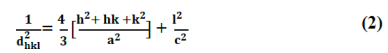
In the same way, by using the relationship of dhkl for the hexagonal system and inclusion of miller indices for the planes (002) and (101), we have deduced the appropriate lattice constants a and c [48] as follows using (Eqs. 2, 3 and 4);


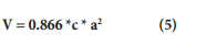
The volume (V) of the unit cell for ZnO wurtzite hexagonal system has been calculated using the following formula (Eq.5):
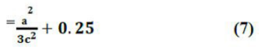
It was found that the volume of unit cell decreases with increasing Ag content. It may be due to decreasing the lattice parameters ‘a’ and ‘c’. When Ag atoms are introduced, there is a change in the electronic bonding between the nearest two atoms which affect the Zn–O bond length. The Zn–O bond length (L) is calculated [49] using the following formula (Eq. 6):

With
The variations in lattice parameters, unit cell volume, crystallite size, bond length of Zn1-xAgxO thin films, microstrain and density of dislocations are reported in Tables 1.2 and 3. From the tables,
it is clear that as Ag doping contents increase in SZO thin films annealed under different environment, the lattice constants (a and c), the volume of unit cell and the Zn-O bond length have decreased consequently.
On the other hand, the grain size D values are estimated from (002) diffraction peaks of all SZO thin films, using Debye–Scherer formula (Eq. 8) [50];
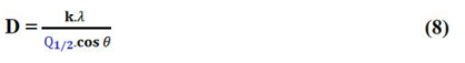
Where λ = 0.15405 nm is the wavelength of Cu Kα radiation, ,𝖰𝟏/𝟐, the full width at half maximum (FWHM) of the main diffraction peak in radian, θ, the Bragg angle and K, the Scherrer’s constant (equal to 0.90 according to the widespread practical).
The evolution of grain size vs various Ag doping concentration and under different annealing treatments environment is illustrated in Figure 4. As compared to undoped ZnO, the grain sizes of SZO thin films decrease slightly with the increase in Ag doping content noticed especially for films annealed in air and under nitrogen flow. This is in good agreement with the reported result of Liu et al [51], they found that the Ag-doping led to a smaller ZnO grains. However, the grain size of SZO films annealed under oxygen flow has been slightly decreased from 27.63 nm for undoped ZnO to 23.82 nm with low doping concentration 1% and increases with further increase in Ag doping concentration reaching a maximum grain size value around 37.85 nm for 2% Ag doping content.
The microstrain (𝛏), which is an interesting structural parameter of ZnO:Ag spin coated thin films is calculated using the following relation (Eq.9) [52]:

where, 𝖰𝟏/𝟐 is the full-width at half-maximum of (002) peak and 𝜽 is the Bragg angle. The evolution of microstrain vs various Ag doping concentration and under different annealing treatment atmospheres was shown in Figure 5. As illustrated in tables 1, 2 and 3 and Figure 5, the strain values decrease with increasing Ag doping concentrations.
The number of dislocations in a material is defined as the dislocation density (𝛿) which represents the amount of defects in a film. It has been defined as the length of dislocation lines per unit volume or the number of dislocations intersecting a unit area which can be estimated as (Eq. 10)[53];

where n is a factor which is equal to unity giving minimum dislocation density and D is crystallite size.
From this structural study, we point out the fact that the decrease in grain size (D) as well as the increase of both of the strain and the dislocation density are indeed understood as an important role played by the introduction of Ag doping element
Optical Properties
UV- Vis measurements
Transmittance plots of undoped and Ag-doped ZnO (SZO) films deposited onto glass substrates after annealing treatments in air, under nitrogen flow and under oxgen flow are shown in Figures 6,7 and 8.
Undoped ZnO thin films exhibit high transparency in the visible region. The transmittance of all SZO films in the visible region (400 nm-800 nm) is about:
● 70% - 80% for SZO films annealed in air.
● 75% - 80% for SZO films annealed under nitrogen flow.
● 80% - 85% for SZO films annealed under oxygen flow.
It can be seen that the drastic decrease in transmittance corresponds to a sharp absorption edge in the near-UV region (NBE). Also, we can notice the presence of interference fringes which can be attributed to reflections on the surface of the layer at the interface layer/substrate.
The fundamental absorption edge of the films corresponds to transitions of electrons from the valence band to the conduction band edge and this can be used to calculate the difference in the optical band gap of the films. In order to calculate the optical band-gap energy (𝐸𝑔) of SZO thin films, the absorption coefficient can be estimated as (Eq.11) [54]:

Where T and R are the transmittance and reflectance coefficients respectively and d is the film thickness.
For the direct band gap of the ZnO Würtzite structure, its absorption coefficient and band gap obey to the following relationship (Eq.12) [55]:
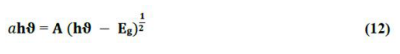
Where A is a constant, hν is the photon energy and Eg is the optical band gap
If one plots (αhϑ)2 vs. photon energy hϑ, optical band gap (Eg) of ZnO and Ag-doped ZnO thin films can be obtained by extrapolating the linear part of the curve to (αhϑ)2 = 0. The related curves for our SZO samples are shown in Figures 9, 10 and 11 and The calculated values of optical band gap (Eg) of Agdoped ZnO thin films annealed under different atmospheres are summarized in Table 4 and depicted in figure 12.
The optical band gaps of undoped ZnO annealed in air and under nitrogen flow fall in the same range at about 3.24 eV. Whereas, the optical band gap of pure ZnO thin film annealed under oxygen flow was found around 3.29 eV. Silver incorporation leads to an obvious decrease in SZO band gaps annealed in these three different atmospheres. In fact, the minimum band gap values were obtained with 3% Ag doping content for SZO films annealed in air (3.22 eV), with low doping content 1% Ag for SZO films annealed under nitrogen flow (3.22 eV) and with 2% Ag doping concentration in case of SZO films annealed under oxygen flow (3.23 eV). The decrease of band gap energy after the incorporation of Ag into SZO thin films annealed under different atmospheres may be attributed to the segregation of Ag atoms to grain boundaries. In fact, these atoms of silver have introduced electron localized states at the ZnO band-gap closer to the lower edge of conduction band forming new lowest unoccupied molecular orbital, which leads in the band gap reduction. The decrease of the band gap with increasing Ag doping in ZnO has been also revealed in several previous reported results [56,57].
Photoluminescence studies
As the exciton binding energy of ZnO is quite high at RT, exciton emission in UV region is possible in ZnO thin films. The photoluminescence spectra of undoped ZnO and Ag-doped ZnO thin films annealed under different atmospheres are recorded at room temperature and shown in Figures 13-15.
A weak violet peak was observed for undoped ZnO films located at about 394.7 nm for films annealed in air, at around 379.82 nm for ZnO thin film annealed under nitrogen flow and at about 377.64 nm for ZnO film annealed under oxygen flow. In literature, there is a consensus that the UV emission of ZnO belongs to the near band edge emission (NBE) since its position is located close to the band gap energy (~ 3.3 eV) of ZnO at room temperature [58] and it was attributed to the radiative recombination of free excitons [39]. However, this UV peak was down shifted to about 377.64 nm for 3% Ag content after silver doping into SZO thin films annealed in air. In addition, this UV peak for SZO films annealed under nitrogen flow was down shifted to about 378.043 nm for 3% Ag doping content. The same trend was also observed with Xue et al [59] in their study concerning the influence of Ag doping on the optical properties of ZnO films.
In case of SZO thin films annealed under oxygen flow, there is a slight shift toward higher UV peak position after Ag doping
The intensity of this UV peak for SZO annealed in air atmosphere has increased as the Ag concentration in the films increased to 1% Ag compared to undoped ZnO films and then decreased as the Ag concentration further increased from 2% to 3% Ag.
In case of SZO films annealed under nitrogen flow atmosphere, the Ag incorporation leads to a gradually increase in UV peak as compared to pure ZnO film which has the minimum intensity. The same behavior of enhanced UV peak intensities for SZO thin films annealed under oxygen flow as compared to pure ZnO film. The intensities of the UV peak for all the SZO films annealed under different atmospheres increase as Ag doping concentration increase and this behavior is in well agreement with the result obtained by Akhilesh Tripathi et al [45] in their study concerning the UV enhancement in polycrystalline Ag-doped ZnO films deposited by the sol– gel method
Table 5 exhibited the band gap values measured from UVVis Transmittance (opt) and from PL measurements. The gap energies of silver-doped ZnO thin films could be derived from optical measurements. All the estimated values are listed in table5.
Therefore, optical band gap energies estimated from UV-Vis transmittance data were found in the range 3.24 eV - 3.22 eV for SZO thin films annealed in air atmosphere. However, Band gap values estimated from PL spectra were slightly modified and fall in the range 3.25 eV – 3.28 eV except the undoped ZnO thin film that have the minimum value of band gap around 3.14 eV. A clearly band gap redshift between (opt) and 𝐸𝑔 (PL) was noted for the whole SZO thin films annealed in air atmosphere. This redshift mainly arises from either intrinsic or extrinsic defects in the film which can easily form recombination centers. Thus, these defects introduce levels inside the band gap of semiconductor material.
The same trend of band gap redshift between (opt) and 𝐸𝑔 (PL) was noted for the whole SZO thin films annealed in both of annealing treatment atmospheres either under nitrogen flow or under oxygen flow.
Conclusion
Silver-doped ZnO thin films have been successfully prepared using sol–gel method onto glass coated glass substrates. The effect of Ag doping content (1, 2 and 3%) on structural and optical properties was investigated. As compared to undoped, It was found that Ag doping leads to a decrease in grain size and band gap values for both of air and nitogen postannealing treatment. However, for oxygen pot-annealing atmosphere grain size was found to increase after Ag incorp oration allowed by a decrease in bad gap. All films are highly transparent in the visible region for different annealing environment. In addition, band gap energies were found to decrease after Ag doping as compared to those of pure ZnO thin films post-annealed in different atmospheres. As compared to pure ZnO thin films, an increase of the photoluminescence intensity was observed.
Acknowledgements
This work was supported by the Ministry of Higher Education and Scientific Research of Tunisia.
References
- Ellmer K, Klein A, Rech B (2008) Eds, Springer-Verlag: Berlin Heidelberg Germany. 104: 1-3,
- Bundesmann C, Schmidt-Grund R, Schubert M. In Transparent Conductive Zinc Oxide—Basics and Applications in Thin Film Solar Cells Springer Series in Materials Science.
- Chen JL, Chen D, Chen ZH (2009) Optimization of the process for preparing Al-doped ZnO thin films by sol-gel method. Sci China Ser E Tech Sci 52: 88-94,
- Tseng YK, Gao GJ, Chien SC (2010) Thin Solid Films 518: 6259-6263.
- Pearton SJ, Norton DP, Ip K, Heo YW, Steiner T, Vac J (2004) Sci Technol B 22: 932-948.
- Lupan O, Shishiyanu S, Ursaki V, Khallaf H, Chow L, et al. (2009) Sol Energy Mater Sol Cells 93: 1417-1422.
- Von Wenckstern H, Schmidt H, Brandt M, Lajn A, Pickenhain R, et al. (2009) Prog Solid State Chem 37: 153-172.
- Znaidi LT, Touam D, Vrel N, Souded S, Ben Yahia O, et al. (2013) Boudrioua Coatings 3: 126.
- Gurav KV, Gang MG, Shin UM, Patil PR, Deshmukh GL, et al. (2014) ctuators B: Chem 190: 439.
- L, Tang S, Yang Z, Wang B (2013) Zhou Ceram Int 39: 5771-5776.
- Shinde SS, Bhosale CH, Rajpure KH (2013) Photochem Photobiol. B: Biol 120: 1.
- Tarwal NL, Devan RS, Ma YR, Patil RS, Karanjkar MM, Patil PS (2012) Electrochim Acta 72: 32.
- Dridi D, Bouaziz L, Karyaoui M, Litaiem Y, Chtourou R (2018) J Mater Sci-Mater El 29: 8267-8278.
- Thongsuriwong K, Amornpitoksuk P, Suwanbon S (2012) Sol-Gel Sci Thechnol 62: 304.
- Wang T, Wu H, Wang Z, Chen C, Liu C (2012) Appl Phys Lett 101: 161.
- Abdulgafour HI, Hassan Z, Ahmed NM, Yam FK (2012) J Appl Phys 112: 074.
- Zhang H, Shen R, Liang H, Liu Y, Liu Y, et al. (2013) Phys D Appl Phys 46: 65.
- Wanga M, Kim EJ, Hahn Lumin SH (2011) 131: 1428.
- Wang LW, Wu F, Tian DX, Li WJ, Fang L, et al. (2015) Zhou Alloy Comp 623: 367.
- Xu L, Fang GU, Jing SU, Chen Y, Li X, Wang X (2011) Alloy, Comp, 509 2942.
- Yuan H, Xu M, Huang QZ (2014) Alloy Comp 616: 401.
- Tarwal NL, Gurav KV, Mujawar SH, Sadale SB, Nam KW, et al. (2013) Ceram Int.
- Wang ZL (2012) Adv Mater 24: 4632.
- Singh N, Kumari B, Sharma S, Chaudhary S, Upadhyay Vibha R, et al. (2014) Energ 69: 242
- Yu S, Zhang W, Li L, Dong H, Xu D, Jin Y (2014) Appl Surf Sci.
- Sutanto H, Wibowo S, Nurhasanah I, Hidayanto E, Hadiyanto H (2016) Int J Chem Eng.
- Sutanto H, Nurhasanah I, Hidayanto E (2015) Mater Sci Forum 827: 3-8.
- Badawy MI, Mahmoud FA, Abdel-Khalek AA, GadAllah TA, Abdel Samad Desalin AA (2014) Water Treat 52: 13-15.
- Lanjewar M, Gohel Inorg JV (2016) Nano-Metal Chem 47: 1090-1096.
- Singh N, Choudhary S, Upadhyay S, Satsangi VR, Dass S, Shrivastav R (2014) Solid State Electrochem 18: 523-533.
- Tarwal NL, Patil PS (2011) Electrochim Acta 56: 6510- 6516.
- Li WJ, Kong CY, Ruan HB, Qin GP, Huang GJ, et al. (2012) Fang Solid State Commun 152: 147-150.
- Yung-Chen, Cheng Kai-Yun, Yuan Miin-Jang Chen (2016) Alloy Comp 685: 391.
- Xu L, Zheng G, Wanga J, Xian F, Liu Y (2016) Optik 127: 5942-5949.
- Thomas MA, Sun WW, Cui JB (2012) Phys, Chem, C 116: 6383.
- Lu YM, Li XP, Su SC, Cao PJ, Jia F, et al. (2014) Zhu Lumin 152: 254.
- Xu L, Zheng G, Zhao L, Pei S (2015) Lumin 158: 396.
- Touam T, Boudjouan F, Chelouche A, Khodja S, Dehimi M, et al. (2015) Boudrioua Optik 126: 5548.
- Boudjouan F, Chelouche A, Touam T, Djouadi D, Khodja S, et al. (2015) Lumin 158: 32.
- Lee DH, Park KH, Kim S, Lee SY (2011) Thin Solid Films 520 1160.
- Karunakaran C, Rajeswari V, Gomathisankar P (2011) Superlattices Microstruct 50: 234.
- Jin Y, Cui QY, Wang K, Hao J, Wang Q and Zhang J (2011) Appl Phys 109: 053521.
- Xiang Q, Meng G, Zhang Y, Xu J, Xu P, Pan Sens Q (2010) Actuator B: Chem 2: 635.
- Dridi D, Yousra Litaiem, Karyaoui M and Chtourou R (2019) Eur Phys J Appl Phys.
- Tripathi A, Prakash Misra K, Shukla RK (2014) Lumin 149: 361-368.
- Karki B, Nakarmi JJ, Singh RB, Banerjee M (2018) Inst Sci Tech 22: 2469.
- Bragg WL (1913) Proceedings of the Cambridge Philosophical Society 17: 43-57.
- Peng LP, Fang L, Yang XF, Li YJ, Huang QL, Wu F, et al. (2009) J Alloys Compd 484: 575-579.
- Chand P, Gaur A, Kumar A (2013) Superlattices Microstruct 64: 331-342.
- Tripathi R, Kumar A, Bharti C, Sinha TP (2010) Curr Appl Phys 2: 676-681.
- Liu K, Yang B, Yan H, Fu Z, Wen M, et al. (2008) Appl Surf Sci 255: 2052.
- Sahay PP, Nath RK (2008) Sens Actuators B 134: 654- 659.
- Saleem M, Fang L, Wakeel A, Rashad M, Kong CY (2012) World J Condens Matter Phys 2: 10-15.
- Rmili A, Ouachtari F, Bouaoud A, Louardi A, Chtouki T, et al. (2013) J Alloys Compd 557: 53-59.
- Zebbar N, Aida MS, Hafdallah A, Daranfad W, Lekiket H, Kechouane M (2009) Mater Sci Forum 609: 133-137.
- Karyaoui M, Mhamdi A, Kaouach H, Labidi A, Boukhachem A, et al. (2015) Mater Sci Semicond Process 30: 255.
- Sahu DR (2007) Microelectron 38: 1252.
- Garcia MA, Merino JM, Ferna´ndez Pinel E, Quesada A, de la Venta J, et al. (2007) Hernando Nano Lett 7: 14-89.
- Xue H, Xu XL, Chen Y, Zhang GH, Ma SY (2008) Appl Surf Sci 255: 1806.
Artcle Information
Review Article
Received Date: February 05, 2026
Accepted Date: February 20, 2026
Published Date: February 22, 2026
Effect of Annealing Treatment Atmosphere on the Structural and Optical Properties of Silver Doped Zinc Oxide Thin Films
Volume 1 | Issue 1
Citation
Dridi D, Litaiem Y, Karyaoui M, Dimassi W and Chtourou R (2026) Effect of Annealing Treatment Atmosphere on the Structural and Optical Properties of Silver Doped Zinc Oxide Thin Films. J Chem Reac Catal Res 1:105
Copyright
©2026 Dridi D. This is an open-access article distributed under the terms of the Creative Commons Attribution License, which permits unrestricted use, distribution, and reproduction in any medium, provided the original author and source are credited.

doi: jcrc.2026.1.105