

Review Article
Volume-1 Issue-1, 2026
Highly compacted and stable CdSe/TiO2 electrodeposited heterostructure for improving simultaneous photoelectrochemical and photocatalytic performances
-
Received Date: January 15, 2026
-
Accepted Date: January 28, 2026
-
Published Date: January 31, 2026
Journal Information
Abstract
In this work, highly compacted and stable Cadmium Selenide/Titanium Dioxide (CdSe/TiO2) heterostructure has been designed through a low cost and easy electrochemical deposition strategy for improving simultaneous photoelectrochemical and photocatalytic performances. At one step, TiO2 layers were deposited onto indium doped tin oxide (ITO) conductive glass substrates by sol-gel via spin-coating method. At a second step, the prepared TiO2/ITO sample was used as working electrode for the CdSe electrodeposition approach from ionic liquid/organic solvent (tri-noctylmethyl-ammonium chloride (TOMAC))/ Formamide (FA) based electrolyte. Structural, morphological,optical, photoelectrocemical (PEC) and photocatalytic properties of bare TiO2 and CdSe/TiO2 photoanodes (PAs) have been studied. Raman analysis confirms the obtained X-Ray Diffraction results by exhibiting the characteristic peaks for the anatase type and hexagonal phase of TiO2. Morphological investigation by Atomic force microscopy (AFM) shows a dense, homogeneous and a surface covered with well distributed small spherical shaped grains for bare TiO2 layer. Its root mean square (RMS) surface roughness has rised from 1.08 nm to 38.833 nm after electrodeposition of CdSe. In order to confirm these AFM results, scanning electron microscopy investigation reveals a surface clearly filled with granular shapes for bare TiO2 layer. Then, the morphology has been modified and consisting of well distributed and agglomerated small grains on the surface of TiO2 resulted from the growth of CdSe film. As compared to bare TiO2,optical measurements show better charge separation efficiency for the CdSe/TiO2 heterostructure. The electrodeposition of highly compacted CdSe onto TiO2/ITO has resulted in enhanced photocurrent density of 0.30 mA/cm2 at 0.5V which is 7.5 times higher than bare TiO2 when exposed to visible light irradiation. The sensitization process of TiO2 with CdSe has also improved photocatalytic degradation efficiency of TiO2 towards Methlylen Blue and Methyl Orange pollutant dyes thanks to the enhancement of its absorption capacity and charge separation rate of photogenerated carriers. The sensitization of TiO2 with CdSe has resulted in a low cost and high stable CdSe/TiO2 promising photoanodes for both of PEC based solar cells and photocatalytic degradation applications and consequently ccould overcome the serious environmental issues.
Key words
CdSe/TiO2, Electrodeposition, Sensitization, Electrolyte, Photoelectrochemical performance, Photocatalytic Degradation
Photosensitization approach |
Jsc [mA/cm2]] |
Voc |
FF |
η [%] |
Ref |
CBD |
1.7 |
- |
- |
- |
[17] |
CBD |
12.6 |
0.74 |
44 |
4.14 |
[18] |
CBD |
11.33 |
0.395 |
42.8 |
3.83 |
[19] |
CBD |
10.9 |
0.395 |
49.4 |
2.13 |
[20] |
CBD |
12.1 |
0.45 |
32.1 |
1.75 |
[21] |
CBD |
6.2 |
0.54 |
53 |
1.8 |
[22] |
CBD |
9.74 |
0.49 |
34 |
1.6 |
[23] |
CBD/Silar |
13.6 |
0.57 |
52 |
3.95 |
[26] |
Silar |
4.68 |
0.43 |
24.2 |
0.48 |
[27] |
Silar |
8.16 |
0.58 |
41 |
2.15 |
[28] |
Silar |
9.72 |
0.492 |
47 |
2.26 |
[29] |
Silar |
10.32 |
0.517 |
49 |
2.65 |
[30] |
Electrodeposition Conditions |
Electrolyte |
PEC measurements |
Ref |
potentiostatic electrodeposition; |
Aqueous solution; [CdCl2]= 0.2 M |
At tdep= 30 s, Jsc, max = ~ 1mA/cm2 |
[31] |
Pulse electrodeposition; applying square pulse potential of -0.85 V as on-potential and 0.00 V as off-potential voltages duty cycles varying from 10 %, 25 %, 50 %, 75 |
aqueous solution; |
At 50 % duty Cycle, Jsc, max = |
[32] |
2 cyclic voltammetry |
Aqueous solution; [CdCl2·5H2O]=0.1M |
At [SeO2]= 4 mM SeO2, Jsc max= |
[33] |
potentiostatic electrodeposition; |
Aqueous bath; [SeO2] = 5 mM, |
At pH 3.0, Jsc max= 2.13 mA/cm2 vs Ag/AgCl; Voc, max =-1.05 V under halogen light irradiation (300 W) |
[34] |
Cyclic voltammetry with 2 cycles |
Aqueous bath; |
At pH = 3, Jsc, max = 4.0 mA/cm2 at 0.5 V(vs SCE), 7 times higher |
[35] |
potentiostatic electrodeposition; |
Aqueous bath; |
Upon annealing treatment |
[36] |
IApp = −0.3 mA/cm2 |
Organic bath; [Se] = 5 Mm [CdCl2]= 10 mM |
At tdep=500 s, Jsc,max= 2.1 mA/cm2 at 0 V (vs Ag/AgCl) under visible |
[37] |
|
JSC (mA/cm2) |
Voc (V) |
FF |
η (%) |
TiO2 |
0.04 |
-0.47 |
0.39 |
0.03 |
CdSe/TiO2 |
0.20 |
-0.56 |
0.43 |
0.13 |
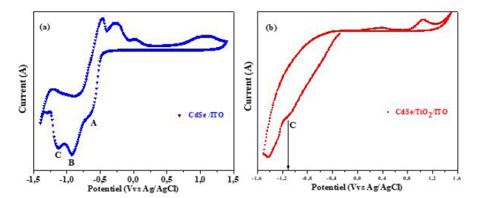 |
| Figure 1: Cyclic voltammograms recorded for binary Cd-Se system from ionic liquid solution composed of 30 % aliquat 336 (TOMAC) and 70 % formamide, 10-2 M SeO2 , 10-2 M CdCl2 and 0.1 M KCl deposited on a) ITO glass substrate, b) ITO/TiO2 working electrodes |
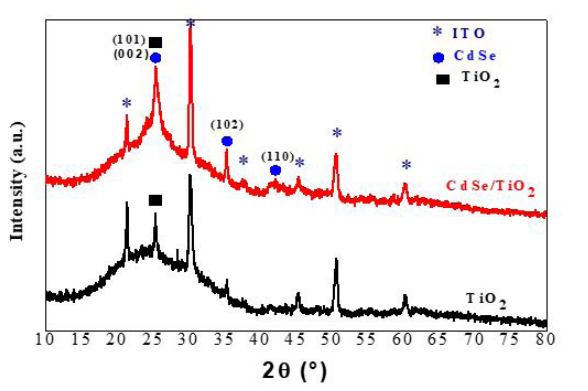 |
| Figure 2: X-ray diffraction patterns of bare TiO2 and CdSe/TiO2 thin films |
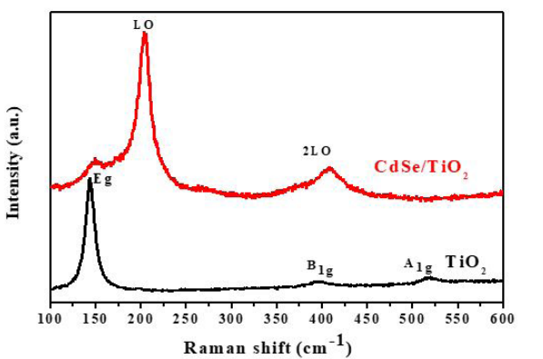 |
| Figure 3:Raman spectra of TiO2 and CdSe/TiO2 based thin films |
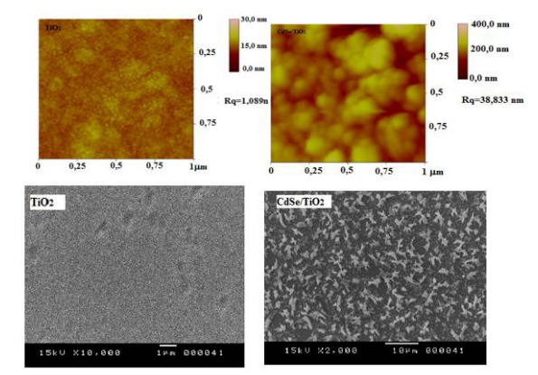 |
| Figure 4: 2D AFM and SEM images of TiO2 and CdSe/TiO2 elaborated thin films |
 |
| Figure 5: UV-vis absorption spectra of TiO2 and CdSe/TiO2 thin films |
 |
| Figure 6: Photoluminescence spectra of CdSe and CdSe/TiO2 thin films |
 |
| Figure 7: Energy levels diagram and schematic illustration of the injection of electrons from the CdSe conduction band to that of the TiO2. |
 |
| Figure 8: Photocurrent density plots of TiO2 and CdSe/TiO2 photoanodes in dark (A) and under illumination (100 mW/ cm2) (B) |
 |
| Figure 9: Schematic illustration of the PEC water splitting for the CdSe/TiO2 photoelectrode |
 |
| Figure 10: Photoconversion efficiency of bare TiO2 and CdSe/TiO2 photoanodes as a function of applied potential |
 |
| Figure 11: Photocurrent density-time response of TiO2 and CdSe/TiO2 photoanodes under illumination (100 mW/cm2) at an applied potential of 0 V (vs Ag/AgCl) |
 |
| Figure 12: Absorption spectra of Methylene blue (a) and Methyl orange (b) solutions obtained after 2 h in the presence of TiO2 and with CdSe/TiO2 photocatalysts |
Introduction
Thanks to Fujishima and Honda discovery related to the solar driven photocatalytic splitting of water on TiO2 photoelectrodes in the early 1970s [1], photocatalytic and photoelectrochemical processes have been widely emerged as low cost and efficient environmental key solutions to tackle serious energy crisis and worldwide pollution issues [2,3]. Despite the outstanding features of TiO2 including its eco-friendliness, cost-effectiveness, robustness, corrosion stability, high electrical and optical properties and strong photocatalytic activity [4,5], its wide band gap of 3.0eV for rutile and 3.2eV for anatase has severely affected its photoresponse which get limited to only 5% in the ultraviolet region of sunlight energy and resulted in lower photoconversion efficiency due to the high recombination rates of photogenerated eloctron-hole pairs [6]. In order to adress that issue, several strategies have been investigated to extend the light response field of TiO2 to visible light and minimizing the recombination rates of the photoexcited charge carriers through doping [7-10], surface modification [11,12] and coupling TiO2 with narrow band-gap semiconductors [13-15]. In particular, nanostructured II–VI semiconductors based on cadmium chalogenides are globally used as light harvesters such as cadmium telluride and cadmium selenide thanks to its high values of absorption coefficient.
Precisely, Cadmium Selenide, named also cadmoselite (CdSe) earned recognizable interest as noteworthy active material to alter TiO2 thanks to its exclusive and special properties namely its reduced band gap (1.7 eV) near to visible spectrum, high absorption coefficient, n-type conductivity, low resistivity, luminescent properties and its direct and reduced band gap around 1.73 eV which is characteristic of the solar spectrum radiation [16]. To date, huge research efforts have been conducted on seeking for the best and low cost technology to sensitize TiO2 with CdSe for improving photoelectrochemical performance. By doing a literature survey, several research groups have extensively proposed either chemical bath deposition strategy [17-26] or SILAR approach [26-30] for the CdSe sensitization of TiO2 and reported its effect on photoelectrochemical performance (Table1). However, these two direct deposition techniques have restricted application in coating onto substrates and consume long deposition time. Thereby, it is necessary to establish a low cost and simple strategy for the design of highly efficient CdSe/ TiO2 photoanodes. Interestingly, electrodeposition method has owned huge interest in recent years since it has numerous advantages including its low cost of synthesis, its environmentally friendly, its simple operating conditions, efficiently adjustability of different parameters like temperature, chemical composition, morphology, area and thichness, last but not least it produces CdSe films at a very high yield.
Thus far, plenty of research groups have investigated the impact of various deposition parameters during the electrolysis process on the possibility to achieve enhanced photoelectrochemical performance of high controlled electrodeposited CdSe/TiO2 photoanodes such as the deposition time, electrolyte’s pH, type of electrolyte and the annealing treatment temperature (Table 2). In fact, Wang et al 2015 [31] reported potentiostatically electrodeposition of CdSe onto anodized TiO2 nanotube arrays. (NTAs) at various deposition time (30s, 35, 25s, 20s and 60s). They concluded that the deposition time of 30 s displayed excellent PEC performance by exhibiting a maximum photocurrent intensity of ~1 mA/cm2 versus saturated calomel electrode (SCE) under visible light irradiation at 0.5 V. They ascribed this result to the high dispersity of CdSe nanoparticles on both inside and outside of the TiO2 NTAs pore walls, the strong combination and heterojunctions between CdSe and TiO2 through Cd-O bonds. In 2018, Ayal’s research group [32] have synthesized CdSe / TiO2 heterostructure through pulse electrodeposition method and studied the effect of different duty cycles varying from 10 % to 90 % on photoelectrochemical properties. They found that duty cycles played a crucial role in the formation of CdSe nanoparticles. The maximum photocurrent was evaluated to be 1.94 mA/cm2 vs Ag/AgCl which has been obtained at a duty cycle of 50 %. The reached photoconversion efficiency was 1.18% which is 59 times higher than nude TiO2. In 2013, Xue and co-workers [33] have prepared photoabsorbing CdSe electrodeposited films onto anodized TiO2 from an acidic bath and studied the effect of the SeO2 concentration (0, 2, 4, 6, 8 and 10 mM). on the PEC performance. At a precise SeO2 content of 4 mM shows a maximum photocurrent of 7.72 mA/cm2 vs SCE under visible light irradiation with a Voc value of 1.24 V and an optimum efficiency of 7.1 %. In 2016, the same group of Ayal [34] have potentiostatically electrodeposited CdSe layer onto TiO2 filmsand reported the effect of various pH values (1.0, 2.0, 3.0 and 3.3) on its PEC performance. The maximum photocurrent density of 2.13 mA/cm2 vs Ag/AgCl under halogen light irradiation was reported at a pH of 3. The highest photoconversion efficiency was 1.02 % which is 51 times higher than bare TiO2 nanotube array. This enhanced photoresponse may be due to the formation of well crystallized CdSe nanocrystals which were well bonded with TiO2. In 2014, Xue and his colleagues [35] have investigated the impact of electrolyte’s pH on PEC performance of electrodeposited CdSe on TiO2 layers. They have varied the pH values from 1 to 4 and they found that pH value of 3 has exhibited the maximum photocurrent density around 4.0 mA/cm2 at 0.5 V (vs SCE) which is 7 times higher than bare TiO2 NTAs and a Voc of -1.26 V. In 2017, Ayal’s team work [36] have investigated the effect of thermal annealing on the enhancement of PEC properties of electrodeposited CdSe onto anodized TiO2. They deduced that annealing treatment play an important role in controlling the formation of CdSe nanoparticles on TiO2. The highest photocurrent density and photoconversion efficiency achieved values were 2.98 mA/cm2 vs Ag/AgCl and 1.67 % respectively obtained at an annealing temperature of 250 °C
In 2019, Zhuang et al [37] were the first to publish the electrodeposition of CdSe photosensitizers onto TiO2 films from an organic bath of N,N-dimethylformamide (DMF) and studying the effect of deposition time on the PEC properties of elaborated CdSe/TiO2 photoanodes. At a deposition time of 500 s, enhanced photoelectrochemical (PEC) performance was achieved with a significant saturated photocurrent density of 2.1 mA/cm2 at 0 V (vs Ag/AgCl) under visible light irradiation (λ ≥ 420 nm). They attributed this enhancement to the good distribution of CdSe nanoparticles on TiO2 nanorod arrays, the favorable band alignment, and the intimate interfacial interaction between CdSe nanoparticles and TiO2 nanorods.
Based on literature, the electrodeposition of CdSe onto TiO2 films could be applied from various types of electrolytes including aqueous solutions [31-36], organic solutions [37] or ionic liquid medium. In fact, ionic liquids are molten salts with melting points often around 20–25 °C or below, composed only of ions. As compared to acqueous and organic electrolytes, ionic liquids are much preferred thanks to its high thermal and good electrochemical stability (> 300 ◦C) Which permitting the electrodeposition to be proceeded even at high temperatures allowing atom diffusion on the surface during growth. It has crucial positive impact on the quality of the resulted layers. ILs exhibit good solvating properties, high conductivity, nonvolatility, low toxicity and wide electrochemical potential window. The viscosity of ionic liquids causes a slowdown electrocoating giving a more homogeneous and compact thin films. Another important advantage of ILs based electrolyte is the absence of hydrogen evolution simultaneously with metal deposition that often occurs during electrodeposition in aqueous solution. This phenomenon has a deep effect not only on photocurrent efficiency but also on the final quality of deposited layer. Thus, Ionic liquids (ILs) were considered as an appropriate alternative electrolytes for the electrodeposition of CdSe onto TiO2 thanks to their intrinsic physico-chemical properties [38,39]. Actually, There are no published work reported the effect of the ionic liquid based electrolyte or ionic liquid/ organic solvent based electrolyte medium on the PEC performance of electrodeposited CdSe films on to TiO2 films.
In this work, we report for the first time ever on the simple and low cost electrochemical deposition strategy of CdSe onto solgel prepared TiO2 thin film from Tricaprylmethylammonium chloride/Formamide based electrolyte as eventual mixture of (Ionic Liquid/ Organic Solvent) medium. Then, the effect of TiO2 sensitization with the electrodeposition of CdSe layer on structural, optical, photoelectrochemical and photocatalytic properties has been deeply investigated.
Experimental Details
Materials
All chemicals were of analytical reagent grade, purchased from Sigma Aldrich and were used without further purification. Aqueous solutions were prepared using deionized water. Sol-gel via spin coating method was adopted to deposit the TiO2 thin films onto ITO conductive glass substrates. Prior to use, all substrates were ultrasonically cleaned during 15 min with consecutively acetone and iso-propanol, rinsed with deionized water, and finally dried in air at room temperature. The CdSe was deposited by electrodeposition technique on TiO2 electrode
Preparation method of TiO2
TiO2 thin films were prepared using sol–gel process and then deposited on ITO glass. Titanium isopropoxide Ti(OCH(CH3)2)4 was used as a TiO2 source. The sol was a mixture, in a molar ratio, of titanium isopropoxide, as a precursor, isopropanol CH3CH(OH)–CH3 and methanolCH3OH, as solvents and acetic acid CH3COOH as a catalyst. First, 1.5 mL of Ti(OCH(CH3)2)4 was dissolved in 4.5 mL of isopropanol. The solution was homogenized for 30 min under magnetic stirring while heating up to 60 °C. Then 4 mL of acetic acid was added, with stirring for 30 min under the same heating. Finally, heating was stopped and 12 mL of methanol was added. The mixture was held under the magnetic stirring for 2 h. The TiO2 was deposited onto (ITO)-coated glass substrates by using spin coating technique. The spinning speed was set at 3000 rpm and the deposition time to 30 s. The TiO2 solution was dropped one time onto the substrate and then dried in the oven at 100 °C for 10 min; The drying process was repeated three times and the resulted samples have been annealed at 450 °C for 2h.
Electrodeposition of CdSe onto TiO2 thin film
CdSe sensitized layer was electrodeposited onto the annealed TiO2 thin film at room temperature under agitation from an electrolyte composed of 30 % aliquat 336 (TOMAC) and 70 % formamide, 10-2 M SeO2, 10-2 M CdCl2 and 0.1 M KCl. The electrodeposition was carried out via three-electrodes system (Voltlab PGZ 100) containing TiO2 film as working electrode, Ag/AgCl as a reference electrode, and Pt as a counter electrode. During the electrodeposition, the electrolyte was continuously stirred at a moderate speed with the help of a magnetic stirrer. The deposition potential was fixed at a constant voltage -1.1 volt for about 15 minutes. Finally, the resulted CdSe/TiO2 heterostructure was annealed at 250 °C for 30 min in nitrogen atmosphere.
Characterization of bareTiO2 and CdSe/TiO2 thin films
The samples were characterized by X-ray diffraction (XRD) using Bruker D8 advance X-ray diffractometer with CuKα (λ= 1.541 Ǻ) radiation for 2θ values in the range of 10–80 °. A Raman scattering study was performed on a Jobin Yvon Lab RAM HR spectrometer using 632.8 nm irradiation from a He–Ne laser at (3 mW). Surface morphology of the prepared films was characterized via Atomic Force Microscopy (AFM)(Nano-scope III) in tapping configuration and using a fieldemission scanning electron microscope (FE-SEM, JSM-5410, JEOL). Accelerating voltage of SEM was set to 20 kV. Optical absorption A (λ) of the films was measured by a UV–vis– NIR (Lambda 950) spectrophotometer, equipped with an integrating sphere, in the wavelength range 300–800 nm. Bare TiO2 and CdSe/TiO2 thin films were also characterized by room-temperature photoluminescence spectra (PL) on a PL fluorescence spectrometer (Perkin-ElmerLS55) using a Xe lamp with an excitation wavelength of 300 nm.
Photoelectrochemical measurements
The PEC splitting performance measurements were carried out in a quartz electrolytic cell. The sample (with an average area of 1 cm2), a Pt plate (with an average area of 1 cm2), and an Ag/AgCl electrode were employed as the working electrode, counter electrode and reference electrode respectively. The electrolyte was composed of 0.5 M sodium sulfate aqueous solution. Current densities, as a function of applied potential (-1 to + 0.5 V vs. Ag/AgCl electrode) for the samples, were recorded under front-side illumination with a computer-controlled Potentiostat/Galvanostat PGSTAT30 (Eco Chemie BV) for all PEC experiments. A 300 W Xe short arc lamp passing through an AM 1.5 G filter Model-SS80AA with white light intensity of 100 mW/cm2 was employed to simulate solar light. The intensity of incident light from the Xe lamp was measured using a Photometer Model 70310 from Spectra-Physics.
Key Findings
Electrochemical Growth
In order to determine the deposition potential of CdSe, a systematic cyclic voltammetry study was undertaken on ITO and TiO2/ITO working electrodes from ionic liquid based electrolyte (Figure 1). The potential started at the open circuit potential and was initially swept towards the negative direction at a scan rate of 20 mV/s. From Figure 1(a), three cathodic peaks are clearly seen in the voltammogram at about -0.6 V, -0.9 V, and -1.1V versus Ag/AgCl reference electrode
The deposited cadmium selenide was attributed to the following reactions:

At the beginning, the H2SeO3 (aq) was reduced into H2Se(aq) soluble species. The reduction of H2 Se (aq) to Se0 was started from -0.75 V and reached the peak value at about -0.9 V. Finally, the electrodeposition mechanism of CdSe thin film onto ITO coated glass substrate took place at a potential of -1.1 V versus Ag/AgCl wherein Cd2+ was reduced to Cd on the surface of the substrate. Hence, the CdSe alloy was formed according the potential deposition mechanism [40].
Figure 1 (b) displays the cyclic voltammogram (CV) of electrodeposited CdSe onto TiO2/ITO working electrode from ionic liquid based electrolyte. Obviously, only one main cathodic peak at about -1.1 V versus Ag/AgCl was noted. The change of the cyclic voltammogram CV was attributed to the change in the working electrode’s surface. As compared with Figure 1(a), this main reduction peak was certainly assigned to the electrodeposition of CdSe thin film.
In order to confirm this assumption, the potentiostatic cathodic electrodeposition was conducted at the potential of -1.1 V versus Ag/AgCl onto sol-gel coated TiO2/ITO film. The deposited film was therefore annealed at 250 °C for 30 min in N2 atmosphere and was analyzed by XRD and RAMAN measurements.
Structural study
Figure 2 exibits the XRD patterns of bare TiO2 and CdSe/TiO2 samples. The sol-gel prepared TiO2 layer onto ITO glass substrate via spin coating approach shows a main peak at 25.35 ° which was assigned to (101) plane and attributed to the anatase phase with tetragonal crystal structure of TiO2 (JCPDS #89-4921). This result is in agreement with those published in the literature [41]. The electrodeposition of CdSe onto TiO2/ITO substrate at an applied potential of -1,1 V from the ricaprylmethylammonium chloride/Formamide based electrolyte, additional characteristic peaks have appeared at 2θ = 25.5 °, 35.2 °, and 41.9 ° which were attributed to (002), (102) and (110) planes respectively. These noticeable planes were ascribed to the hexagonal structure of CdSe according to the card number (JCPDS # 65-3415) verified by JCPDS (Joint Committee on Powder Diffraction Standards) database. This structural study reveals that the hybride CdSe/TiO2 nanostructure has been successfully prepared by the low cost and facile electrodeposition approach at the applied potential of -1.1 V.
Raman study
The Raman spectra of bare TiO2 and CdSe/TiO2 films in the range of 100 cm-1 to 550 cm-1 are shown in Figure 3. Solgel coated TiO2 spectrum reveals three symmetric vibration modes; A1g, B1g and Eg attributed to the tetragonal anatase phase of TiO2. They were identified at 144 cm-1 for Eg mode, 396 cm-1 for B1g mode and 516 cm−1 for A1g vibrational mode respectively [42]. The electrodeposition of CdSe onto TiO2 film resulted in the decrease of anatase characteristic peak intensity of TiO2 (Eg) due to the surface recovery of TiO2. In addition, two new peaks have appeared at 203 cm-1 and 406 cm-1 corresponding to the longitudinal optical (LO) and to the second harmonic (2 LO) respectively of CdSe [43]. Those Raman results confirm those obtained by XRD study.
Morphological studies
Figure 4 shows the morphology of bare TiO2 and CdSe/TiO2 films by Atomic Force Microscopy (AFM) and Scanning Electron Microscopy (SEM). The surface of sol-gel coated TiO2 film was dense, homogeneous and covered with well distributed small spherical shaped grains showing the general characteristic morphology of the anatase phase [44]. However, the surface topography has changed after the electrodeposition of CdSe which could be attributed to the CdSe deposited layer onto TiO2 thin film. The root mean square (RMS) surface roughness of nude TiO2 thin film has increased from 1.08 nm to 38.833 nm after electrodeposition of CdSe. The increase in the film roughness has proved the growth of electrodeposited CdSe onto nanostructured TiO2 based thin film. In order to confirm this AFM results, SEM topography has also been investigated in Figure 4.
SEM image of bare TiO2 layer reveals that the surface was clearly filled with granular shapes. After CdSe electrodeposition, the morphology has changed and consists of agglomerated small grains well distributed on the TiO2 surface resulted in the growth of CdSe film
Optical properties
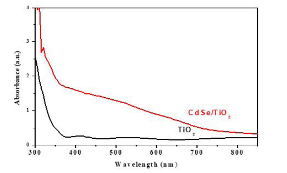
UV-Visible absorption spectra of TiO2 and CdSe/TiO2 thin films are shown in Figure 5. The bare TiO2 has an absorption edge at around ∼375 nm, showing a fundamental absorption edge which corresponds to the TiO2 band gap energy of anatase structure (3.2 eV) in the ultraviolet region [45, 46]. The electrochemical deposition of CdSe onto TiO2 has obviously extended the absorption spectrum to the visible light region. The narrow band-gap of photoabsorber CdSe was responsible for the improved absorption capability of TiO2 thin film in the visible-light region and consequently enhances its photocatalytic and photoelectrochemical performances [47].
The charge separation and transfer mechanism was revealed by measuring the electron injection efficiency by photoluminescence (PL) spectroscopy as shown in Figure 6. Through an excitation wavelength of 300 nm, the CdSe based photosensitizer exhibited a characteristic emission peak situated at 600 nm which corresponds to the recombination of the excited electrons. Whereas, the PL signal disappears with sensitization of TiO2 with CdSe. This PL quenching reveals the decrease in the rate of excited electrons which get recombined radiatively with the holes situated in CdSe valance band. Therefore, it can be concluded that most of the excited electrons are successfully injected into the TiO2 conduction band [48-51].
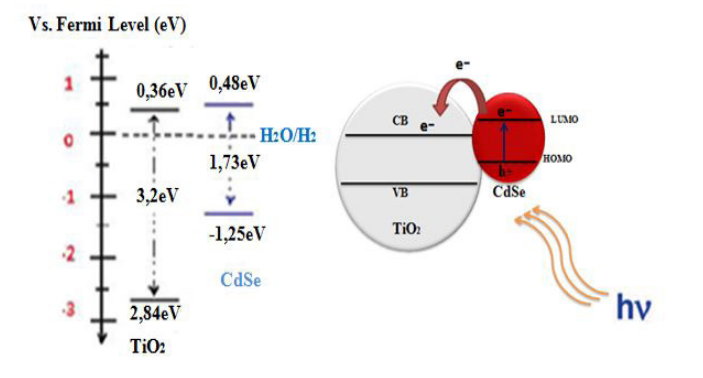
According to the literature, photoluminescence spectroscopy confirms the presence of the type-II interfacial transition between the valence band of CdSe and the conduction band of TiO2 [52, 53] thanks to its energy levels shown in Figure 7. [52- 54]. This PL results suggest that electrodeposition of CdSe onto TiO2 photoelectrode enhances the charge separation
Photoelectrochemical properties
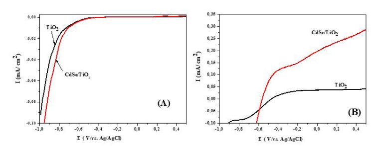
The linear sweep voltammogram (LSV) is a useful technique evaluate the charge carrier characteristics at the semiconductor/ electrolyte interface by evaluating the separation efficiency of photogenerated electron-hole pairs. In order to investigate the impact of the photosensitization of TiO2 with CdSe on the separation efficiency of photogenerated electron–hole pairs, we expose the elaborated photoanodes to a photocurrent response measurements. Figure 8 (A) and Figure 8(B) show current density-voltage (J−V) measurements of TiO2 and CdSe/TiO2 photoanodes in dark and under illumination with 100 mW/cm2 from Xenon lamp in aqueous solution containing 0.5 M Na2SO4 (pH=7) with applied potential ranging from -1 to 0.5 V (vs. Ag/AgCl).
It is clearly seen in Figure 8 (A) that there is no dark photocurrent for both photoelectrodes.
According to a literature survey, this result could be explained by the presence of the TiO2 based compact film that plays an effective role in blocking the direct contact between the electrolyte and ITO substrate which suppresses the leakage photocurrent [54]. The use of TOMAC/FA as ionic electrolyte in the electrodeposition of CdSe onto TiO2/ITO substrate has a crucial positive impact on the quality of the resulted photoanodes by improving the compactness of the film [54]. Under illumination, the increase at applied voltage (V vs.Ag/AgCl) promotes the separation of photo-generated charges and the photo-current density (JSC) has increased [55, 56]. All samples have a common behavior; a photocurrent flowed in the positive potentials and increased gradually which is the characteristic of n-type semiconductor.
Moreover, low photocurrent was observed for the both photoanodes. This may be explained by the fast recombination of the photogenerated electrons and holes. Similar behavior was also reported by others authors [57,58]. Under illumination, bare TiO2 presents a photocurrent density of 0.04 mA/cm2 at 0.5 V which is comparable to that reported by Ayal et al [34], in CdSesensitization of TiO2 nanotube arrays through electrodeposition approach. They have found a 0.03 mA/cm2 as photocurrentdensity for bare TiO2.
As compared to TiO2 layer, the photocurrent density of hybrid CdSe/TiO2 heterostructure was greatly enhanced and reached a value of 0.30 mA/cm2 at 0.5 V which is 7.5 times higher than bare TiO2 We have also noticed from Figure 10(B) that CdSe/TiO2 PA shows a more negative zero-current potential (-0.56V) than that of the bare TiO2 thin film (-0.46 V). These results could be explained through the high absorption and the better charge separation efficiency of the photogenerated carriers [59]. These results are consistent with the Photoluminescence results. This suggests that the electrodeposition of CdSe on TiO2 thin film has improved the generation and separation of photoinduced charges.
Figure 9 shows the PEC water splitting device for the CdSe/ TiO2 PA. Through coupling the two semiconductors, most of the excited electrons have been successfully injected from the CdSe conduction band into that of TiO2. This reduces the photogenerated carriers recombination rate in TiO2. Consequently, it facilitates the transport of electrons to the platinum electrode through the external circuit to participate in the reduction of protons at the interface between the cathode and the electrolyte leading to the formation of hydrogen gas. Meanwhile, the holes generated vacancies and contribute to the oxidation of water by producing oxygen at the interface between the photoanode and the electrolyte. This PEC water splitting mechanism undergo the following steps:
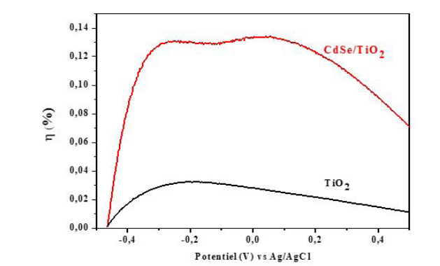
According to the (J-V) curve under illumination, the corresponding photoconversion efficiency, the applied bias photon-to-current efficiency (ABPE) was calculated via the following equation [60] and presented in Figure 10.
where η is the photoconversion efficiency, Jsc is the photocurrent density (mA/cm2), ILight is the incident light, E°rev is the standard reversible potential which is 1.23 V RHE, and Eapp is the applied potential which is Eapp = Emeas − Eaoc, where Emeas is the electrode potential (vs Ag/AgCl) of the working electrode and Eaoc is the electrode potential (vs Ag/AgCl) of the same working electrode under open circuit and under illumination conditions.
The PEC parameters including open-circuit voltages (Voc), shortcircuit current density (Jsc), fill factor (FF) and power conversion efficiency (η) were tabulated in Table 3.
Typically, the CdSe/TiO2 photoanode shows higher conversion efficiency of 0.13 % at -0.2 V (vs Ag/AgCl) which is ~ 4.3 times higher than that of pure TiO2 layer (0.03 %). The enhanced photoconversion efficiency could be assigned to the improvement in incident light absorption and the ameliorated separation rate of photogenerated charges.
In order to investigate the stability and the reproducibility of the device’s phtoresponse, the photocurrent-time (J-t) plots of TiO2 and CdSe/TiO2 photoanodes have been measured at an applied potential of 0 V and displayed in Figure 11. The photocurrent of elaborated samples appeared immediately upon irradiation then quickly returned to a steady state when the illumination was cut off. These results indicate the stability of the samples and the immediate generation and separation of electron (e-)/hole (h+) pairs in TiO2 and CdSe/TiO2 based photoanodes [61]. It is worth noty that the CdSe sensitized TiO2 photoanode yields a photocurrent density of 0.28 mA/cm−2 which is about 9.5 times higher than that reached with bare TiO2 (0.029 mA/cm−2). These results indicated that the sensitization of TiO2 with CdSe can clearly enhance the transient photocurrent responses which confirm the observed trends in Figure 8.
Photocatalytic activities
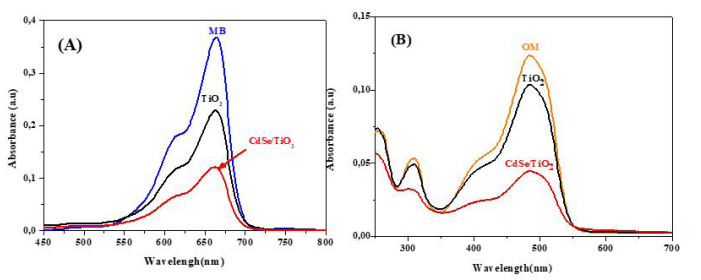
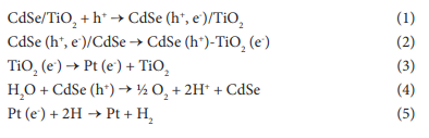
The discharge of untreated wastewater from various industries causes serious environmental pollution and threatens the human and ecosystem well-being. Thus, Methylene blue MB and methyl MO containing wastewater should be decolorized and detoxified before being discharged into the environment since they are potential carcinogen dyes [60-62].
The photocatalytic activities of synthesized photocatalysts were carried out by the degradation of MB and MO dyes under visible light irradiation and illustrated in Figure 12. It is clearly seen that the maximum absorbance of MB and MO dyes situated at 660 nm and 484 nm respectively have sharply decreased in the presence of TiO2 and CdSe/ TiO2 based catalysts. These results show that the photocatalytic degradation efficiency of TiO2 has improved after photosensitization with CdSe. This improvement originated from the enhanced absorption capability and the efficient charge separation [65]. Figure 13.
Conclusion
In summary, the sensitation of TiO2 with short band gap CdSe absorber has successfully provided through the low cost, facile and eco-friendly electrochemical deposition. It has been demonstrated that this electrochemical approach via the use of TOMAC/FA based electrolyte has a crucial role in the high stability and compactness of sol-gel synthesized TiO2 layers.
Structural study proved the cyclic voltammetry synthesis of hybride CdSe/TiO2 nanostructure at the applied potential of -1.1 V with well-defined phases. Meanwile, raman results confirm those obtained by XRD investigation by exhibiting the characteristic peaks for the anatase type TiO2 and hexagonal phase of CdSe respectively. AFM morphological study of bare TiO2 layer shows a dense, homogeneous and a surface covered with well distributed small spherical shaped grains. Its root mean square (RMS) surface roughness has rised from 1.08 nm to 38.833 nm after electrodeposition of CdSe which is a good proof for the successful growth of electrodeposited CdSe onto nanostructured TiO2 based thin film via the TOMAC/FA medium.
In order to confirm this AFM results, SEM image of bare TiO2 layer reveals that the surface was clearly filled with granular shapes.After CdSe sensitization, the morphology has been modified and consisting of agglomerated well distributed small grains on the surface of TiO2 resulted in the growth of CdSe film. As compared to bare TiO2, optical measurements show better charge separation efficiency for the CdSe/TiO2 heterostructure. The sensitization with CdSe has resulted in enhanced photocurrent density of 0.30 mA/cm2 at 0.5 V which is 7.5 times higher than bare TiO2 when exposed to visible light irradiation. In terms of conversion efficiency, CdSe/TiO2 photoanode shows higher conversion efficiency of 0.13 % at -0.2 V (vs Ag/AgCl) which is ~ 4.3 times higher than that of bare TiO2 layer. Also, CdSe/TiO2 PA shows a zero-current potential of -0.56 V which is more negative than that of bare TiO2 thin film (-0.46 V). The sensitization process of TiO2 with CdSe from the ionic liquid has improved photocatalytic degradation efficiency of TiO2 towards MB and MO pollutant dyes thanks to the amelioration of its absorption capacity and charge separation rate of photogenerated carriers. The sensitization of TiO2 with CdSe from TOMAC/FA based ionic liquid medium has resulted in low cost and high stable CdSe/TiO2 photoanode for PEC solar cells and photocatalytic degradation applications and consequently overcome the serious environmental issues
Acknowledgments
This work was supported by the Ministry of Higher Education and Scientific Research of Tunisia.
Conflicts of Interest
The authors declare no conflict of interest.
References
- Fujishima A, Honda K (1972) Nature 238: 37-38.
- Michael A, Henderson A (2011) Surf Science Reports 66: 185- 278.
- Kim HS, Jung SW, Yang SK, Ahn KS, Kang SH (2013) Mater Lett 111: 47-50.
- Huang JY, Zhang KQ, Lai YK (2013) Int J Photoenergy 2013: 761971.
- Mor GK, Varghese OK, Paulose M, Shankar K, Grimes CA (2006) Sol Energy Mater Sol Cells 90: 2011-2075.
- Zhuang H, Miao J, Huang H, et al. (2015) Chem Phys Chem 16: 1352‐1355.
- Zhao H, Chen Y, Quan X, Ruan X (2007) Chinese Science Bulletin 52: 1456-1461.
- Lin HJ, Yang TS, His CS, Wang MC, Lee KC (2014) Ceramics International 40: 10633-10640.
- Tu YF, Huang SY, Sang JP, Zou XW (2009) Journal of Alloys and Compounds 482: 382-387.
- Yang H, Pan C (2010) Journal of Alloys and Compounds 501: 8-11.
- Ma H, Fan Q, Fan B, et al. (2018) Langmuir 34: 7744‐7750.
- Luo Z, Qi Q, Zhang L, Zeng R, Su L, Tang D (2019) Anal Chem 91: 4149‐4159
- Kang Q, Liu S, Yang L, Cai Q, Grimes CA (2011) ACS Applied Materials & Interfaces 3: 746-749.
- Y. Lu, G. Yi, J. Jia, Y. Liang, Applied Surface Science 256 (2010) 7316-7322.
- Z. Zhou, J. Fan, X. Wang, W.Sun, W. Zhou, Z. Du, S. Wu, ACS Applied Materials & Interfaces 3 (2011) 2189-2194
- Aiyun Meng, Liuyang Zhang, Bei Cheng, Jiaguo Yu (2019) Advanced materials 31.
- Chin Wei Lai, Nurul Asma Samsudin, Foo Wah Low, Nur Azimah Abd Samad, Kung Shiuh Lau, et al. (2020) Materials 13: 25-33.
- Hou J, Zhao H, Huang F, Jing Q, Cao H, Wu Q, Peng S, Cao G (2016) J Power Sources 325: 438-445.
- Salunkhe DB, Dubal DP, Sali JV, Sankapal BR (2015) Ceram Int 41: 3940-3946.
- Zhao F, Tang G, Zhang J, Lin Y (2012) Electrochim. Acta 62: 396-401.
- Zhu G, Pan L, Xu, Zhao Q, Lu B, Sun Z (2011) Nanoscale 3: 2188-2193.
- Shen Q, Yamada A, Tamura S, Toyoda T (2010) Appl Phys Lett 97: 123-107.
- Barea EM, Shalom M, Gimenez S, Hod I, Mora-Sero I, Zaban A, et al (2010) J Am. Chem Soc 132: 19.
- Yu L, Li Z, Liu Y, Cheng F, Sun S (2014) J Power Sources 270: 42-52.
- Fang B, Kim M, Fan SQ, Kim JH, Wilkinson DP, et al. (2011) J Mater Chem 21: 8742-8748.
- Liu D, Liu J, Liu S, Wang C, Ge Z, et al. (2019) J Mater Sci 54: 4884-4892.
- Unni GE, Deepak TG, Nair AS (2016) Mater Sci Semicond Process 41: 370-377.
- Wang R, Wan L, Niu H (2013) J Sol-Gel Sci Technol 67: 458-463.
- Zhang Y, Zhu J, Yu X, Wei J, Hu L, Dai S (2012) Sol Energy 86: 964-971.
- Chong LW, Chien HT, Lee YL (2010) J Power Sources 195: 5109-5113.
- Wang W, Li F, Zhang D, Leung DYC, Li C (2016) Photoelectrocatalytic hydrogen generation and simultaneous degradation of organic pollutant via CdSe/TiO2 nanotube arrays. Applied Surface Science. 362: 490-497.
- Ayal AK, Zainal Z, Lim HN, Talib ZA, Lim Y-Chin, Keng CS, Holi AM (2018) Fabrication of CdSe nanoparticles sensitized TiO2 nanotube arrays via pulse electrodeposition for photoelectrochemical application. Materials Research Bulletin. 106: 257-262
- Jinbo Xue, Qianqian Shen, Wei Liang, Xuguang Liu, Fei Yang (2013) Electrochimica Acta 97: 10-16.
- Asmaa Kadim Ayal, Zulkarnain Zainal, Hong-Ngee Lim, Zainal Abidin Talib, et al. (2016) J Mater Sci: Mater Electron 27: 5204-5210.
- . Jinbo Xue, Qianqian Shen, Fei Yang, Wei Liang, Xuguang Liu (2014) Journal of Alloys and Compounds 607: 16
- Asmaa Kadim Ayal, Zulkarnain Zainal, Hong-Ngee Lim, Zainal Abidin Talib, Ying-Chin Lim, et al. (2017) Opt Quant Electron 49: 164.
- Huaqiang Zhuang, Xiaobin Liu, Fukun Li, Wentao Xu, Liqin Lin, Zhenping Cai (2019) Int J Energy Res. 43: 7197-7205.
- Dipal B, PatelaKhushb, Chauhan Mukhopadhyay R (2019) Journal of Electroanalytical Chemistry 847: 113-233
- Shibin Thomas, Jeremy Mallet, Hervé Rinnert and Michael Molinari (2018) RSC Adv 8: 3789.
- Ibtissem Ben Assaker, Halima Elbedoui, Radhouane Chtourou (2012) Electrochimica Acta. 81: 149-154.
- Tu Y, Wu J, Zheng M, Huo J, Zhou P, Lan Z, Lin J, Huang M (2015) Nanoscale 7: 20539-20546.
- Yoshii M, Murata Y, Nakabayashi Y, Ikeda Y, Fujishima M, Tada H (2016) Colloid Interface Sci 474: 34-40.
- Pop LC, Sygellou L, Dracopoulos V, Andrikopoulos KS, Sfaelou S, Lianos P (2014) Catal Today 252: 157-161.
- Legrand-Buscema C, Malibert C, Bach S (2022) Thin Solid Films 418: 79-84.
- Peng YH, Huang GF, Huang WQ (2012) Visible-light absorption and photocatalytic activity of Cr-doped TiO2 nanocrystal films, Advanced Power Technology 23: 8-12.
- Li C, Hsieh JH, Cheng JC, Huang CC (2014) Optical and photoelectrochemical studies on Ag2O/TiO2 double-layer thin films. Thin Solid Films 570: 436-444.
- Wang W, Li F, Zhang D, Leung YC, Li G (2016) Applied Surface Science. 362: 490-497.
- Zhao Q (2015) Applied Surface Science 344: 107.
- Xu J, Yang X, Wang HK, Chen X, Luan CY, et al. (2011) Nano Letters 11: 4138.
- Robel I, Kuno M, Kamat PV (2007) J Am Chem Soc 129: 4136-4137.
- Haonan Ge, Feiyan Xu, Bei Cheng, Jiaguo Yu, Wingkei Ho (2019) Chem Cat Chem 11: 6301-6309
- Van de Walle CG and Neugebauer J (2003) Nature 423: 626- 628.
- Tung Ha Thanh, Dat Huynh Thanh,Vinh Quang Lam (2014) Advances in Opto Electronics 12: 9.
- Joudi F, Chakhari W, Ouertani R, Ben Naceur J, Chtourou R (2018) Journal of Materials Science: Materials in Electroni
- Oliva FY, Avalle LB, Santos E, Cámara OR (2002) Journal of Photochemistry and Photobiology, A: Chemistry 146: 175-188.
- Allam NK, Shankar K, Grimes CA (2008) Journal of Materials Chemistry. 18: 2341- 2348.
- Chakhari W, Ben Naceur J, Ben Taieb S, Ben Assaker I, Chtourou R (2017) Journal of Alloys and Compounds 708: 862- 870.
- Seung Wook Shin, Jeong Yong Lee, Kwang-Soon Ahn, Soon Hyung Kang, Jin Hyeok, Kim (2015) J Phys Chem 119: 13375- 13383.
- Vinodgopal K, Hotchandani S, Kamat PV (1993) Journal of Physical Chemistry 97: 9040-9044.
- Parkinson B (1984) Chem Res 17: 431-437.
- Dai Y, Sun Y (2014) J Mater Chem A 2: 1060-1067.
- Boeningo M (1994) Gov. Printing DNHS (NI0ST-I) publication N°66, Washington DC, U.S, 80-119.
- Prabhakar Y, Gupta A, Kaushik A (2019) Process saf. Environ Protect. 131: 116-126.
- Chen Z, Jin X, Chen Z, Megharaj M, NaiduR () J. Colloid Interface Sci. 361 (2011) 601-663.
- Chi H, Tang W (2013) Mod Res Catal 2: 19-24.
Artcle Information
Review Article
Received Date: January 15, 2026
Accepted Date: January 28, 2026
Published Date: January 31, 2026
Journal of Chemical Reactions and Catalysis Research
Volume 1 | Issue 1
Citation
JOUDI Fedia, DRIDI Donia, LITAIEM Yousra, BEN NACEUR Jamila, DIMASSI Wissem and CHTOUROU Radhouane (2026) Highly and Stable CdSe/TiO2 Electrodeposited Heterostructure for Improving Simultaneous Photoelectrochemical and Photocatalytic Performances. J Chem Reac Catal Res 1:103
Copyright
©2026 DRIDI Donia. This is an open-access article distributed under the terms of the Creative Commons Attribution License, which permits unrestricted use, distribution, and reproduction in any medium, provided the original author and source are credited.

doi: jcrc.2026.1.103